Understanding and controlling the behavior of such domain walls without this new technique is like trying to coach a football game from just two still shots: one showing the quarterback lined up before the snap, and another capturing the moment after the play has ended. Without knowing the events in between, it is much more difficult to know whether the play was a run or a pass, which players were critical or what effort led to the result. Improving how the team plays requires being able to see all the action.
“The method fills in crucial gaps by creating dynamic visualizations that allow scientists to observe how domain walls move and better estimate how much energy is required to shift them. It turns a static snapshot into a vivid, explanatory sequence,” said ORNL’s Stephen Jesse. “Using precisely timed measurement and control electronics, we can rapidly and systematically change the state of a ferroelectric material and watch how changes evolve over time. Until now, this level of detail has not been achieved using atomic force microscopy, and the method can be adapted for use in electron microscopes and other advanced instruments.”
The technique captures both the tiny, repeated movement of domain walls as they react to changes in their environment — such as electric or mechanical signals — and the sudden, stop-and-go movements that happen when the walls are briefly stuck and then abruptly shift, like a door sticking before it swings open.
These patterns of motion, both smooth and jerky, reveal how ferroelectric polarization is modified within the material. Ferroelectric polarization is the natural alignment of electric charges in certain materials that can be changed by an external electric field, and this ability is crucial for applications such as memory storage and sensors.
The researchers aim to further refine this technique to study other materials and collaborate with industry partners to explore potential commercial applications.
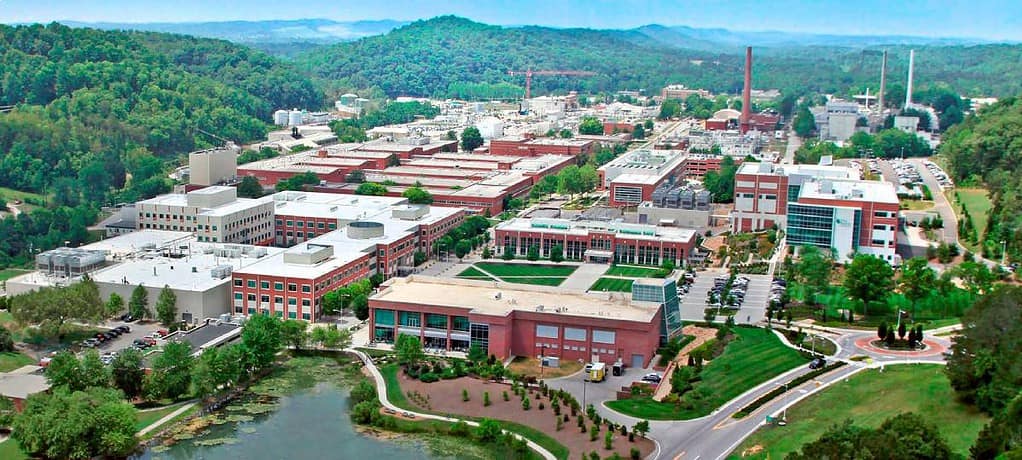
The DOE Basic Energy Sciences program funded this research. The experiments were performed at the Center for Nanophase Materials Sciences, a DOE Office of Science user facility at ORNL.
UT-Battelle manages ORNL for DOE’s Office of Science. The single largest supporter of basic research in the physical sciences in the United States, the Office of Science is working to address some of the most pressing challenges of our time. For more information, please visit energy.gov/science. — Scott Gibson
This Oak Ridge National Laboratory news article "Scientists track tiny structures key to advanced electronics" was originally found on https://www.ornl.gov/news